
サムスンが20nm級 DRAMの量産開始を発表した。
量産する前にサンプル出荷しないと、買う方も設計が詰めれず買えないのにね^^
サムスン発表によると、20nm級は集積度を上げたことで40%コストダウンとのこと。
35nmから40%の面積の圧縮をすると27nmになり、先行するエルピーダの25nmに負けてしまうことになる。
それはさておき、サムスンがDRAMではなく20nm級NAND型フラッシュメモリーの量産発表をしたのだがその経緯を紹介しよう。

世界のサムスン、20nm工程でNAND型フラッシュメモリの量産開始 世界初
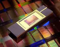
【ソウル時事】韓国のサムスン電子は19日、回路線幅20ナノメートル(ナノは10億分の1)工程で、32ギガビットのNAND型フラッシュメモリーの量産を開始したと発表した。同工程でのメモリー半導体の量産は世界初という。(2010/04/19-12:22)
すまない・・・
そう、
またなんだ・・・
プレスリリースの原文を見て欲しい。
SAMSUNG Producing Industry’s First Higher-performing 20nm-class NAND Flash Memory
Seoul, Korea on Apr 19, 2010 Seoul,
Korea - April 19, 2010 : Samsung Electronics Co., Ltd., the world
leader in advanced semiconductor technology solutions, today announced
the industry"s first production of 20 nanometer (nm) class NAND
chips for use in Secure Digital (SD) memory cards and embedded memory
solutions. Based on this cutting-edge technology, the introduction of 32
gigabit (Gb) MLC NAND will expand the company"s memory card solutions
for smart phones, high-end IT applications and high-performance memory
cards.
Seoul,
Korea - April 19, 2010 : Samsung Electronics Co., Ltd., the world
leader in advanced semiconductor technology solutions, today announced
the industry"s first production of 20 nanometer (nm) class NAND
chips for use in Secure Digital (SD) memory cards and embedded memory
solutions. Based on this cutting-edge technology, the introduction of 32
gigabit (Gb) MLC NAND will expand the company"s memory card solutions
for smart phones, high-end IT applications and high-performance memory
cards.Mr. Soo-In Cho, president, Memory Division, Samsung Electronics, said "In just one year after initiating 30nm-class NAND production, Samsung has made available the next generation node 20nm-class NAND, which exceeds most customers requirements for high-performance, high-density NAND-based solutions." He added, "The new 20nm-class NAND is not only a significant step forward in process design, but we have incorporated advanced technologies into it to enable substantial performance innovation."
Samsung"s 20nm-class MLC NAND has a 50 percent higher productivity level than 30nm-class MLC NAND. The write performance of a 20nm-class-based, eight gigabyte (GB) and higher density, SD card is 30 percent faster than the 30nm-class NAND and it delivers a speed-class rating of 10 (read speed of 20MB/s, write speed of 10MB/s). By applying cutting-edge process, design and controller technology, Samsung also has secured reliability levels comparable to 30nm-class NAND.
Samsung Electronics first began producing 32Gb NAND with 30nm-class process technology in March 2009. Now it is shipping SD card samples to customers that are built with 20nm-class 32Gb NAND and will expand production later this year.
Memory cards based in the 20nm-class will be available from 4GB through 64GB densities
Samsung"s timely introduction of its high-performance premium NAND will better support the growing memory requirements of high-density smartphones, high-end IT applications and high-performance memory cards.
だったんだ・・
20nm級は、2010年4月に量産に入った筈だった。
« 投稿日:: 6月 08, 2011, 01:09:14 午後 » |
同社は、Samsungが4月のプレスリリースで発表した32-Gbitデバイスのように、K9GBG080Aのダイ作成により、チップが27nmの生産プロセス技術に基づき試作されたと特定したと述べている。
UBM TechInsightsによると、これは、20nmクラスで生産された2番目のNANDフラッシュデバイスであり、IM Flash Technologies 製64-Gbit 25nm多層セルNANDフラッシュに結合する。
しかしHynixは、2010年8月に64-Gbit NANDの26nm生産プロセスの量産を行っていると述べている。
さらに同社は、27nmフラッシュは、SDカードアプリケーションに搭載され、書込パフォーマンスは、同じメモリ(Samsung K9GBG08U0M)の35nmバージョンより30%改善されていると示唆している。
総てのメモリサイズの信頼性レベルは、35nmバージョンと互換性がある。メモリのサンプリングは、2010年第3四半期に、量産は2011年第1四半期に開始される。
http://www.bocinfo.biz/forum/index.php?topic=158.msg173#msg173
サムスン27nm NAND型フラッシュメモリチップ製造プロセスの最近リリースされた
UBMはTechInsightsサイトは最近、三星27nm NAND型フラッシュメモリチップ製造プロセスのマイクロチップのようなものだった。
以下は、このNAND型チップ部分の解体です。
に示すように、この内部NAND型フラッシュメモリチップのコアはK9GBG08U0Aの言葉が付いています、このチップは、三星は今年4月にローンチされ、チップのストレージ密度32Gbit 、 27nmプロセス技術を使用して製造。
これは、 20nmのNAND型フラッシュメモリチップの製造プロセス製品に基づき、市場レベルの遠番目の段落によるもので、 64Gbit 25nmのプロセス製品のIMフラッシュの生産の密度である。
しかし、昨年八月には早く、ハイニックスは、 26nmチップ製造プロセスの64Gbit NANDフラッシュメモリ密度の大量生産を持っていると主張しているが、私たちは市場の目の前にチップを見たことがないのかわからない。
UBM
はTechInsightsアナリストは言った:
“サムスンのNANDフラッシュメモリチップが正常に27nmプロセスに35nmのプロセスから進化している、彼らは他の多くのメモリチップメーカーが正
しく解決されていない克服するために、多くの革新的な技術を新しいプロセスで使用されている
問題を修正しました。 “
製品の耐久性は基本的には35nmのプロセス製品と同じですが、この27nm NAND型チップの製造プロセスは、 SDカードで使用する場合、その30%の増加の観点から35nmのプロセス製品(ラベルK9GBG08U0M )に比べてパフォーマンスを書く
。
また、 UBMのTechInsights 、サムスンこの密度27nm 32Gbit NANDフラッシュメモリチップのプロトタイプの仕事昨年の裁判の第3四半期を処理し、大量生産は第1四半期にされていることを指摘された。
テキスト/ドライバホーム
http://www.howaboutchina.com/ja/2011/06/04/samsung-27nm-nand-flash-process-microscopic-analysis-of-recently-released/
本当は2011年の第1四半期だったんだ。
そして市場で確認して報道されたのが2011年6月4日の事だったんだ・・・
さらにそれは20nmなんかじゃなくて27nmだったんだ。
ちなみに、2010年8月にハイニックスが量産に入ったとする26nmは
2011年6月現在で実物が流通していないらしい。